Noise and Interference caused by high-speed digital switching and radiated RF signals can be eliminated by appropriate RF shielding and careful PCB design.
Today’s high-speed digital systems and high-frequency RF circuits are found in everything from cellular phones to high-speed instruments and computer systems. The high-speed subsystems or high-frequency RF circuits radiate significant amounts of electrical interference.
This interference takes the form of both radio-frequency interference (RFI) and electromagnetic interference (EMI), and if left unmitigated, the RFI and EMI can cause system malfunctions, incorrect readings, and other detrimental effects.
To counter the effects, designers can employ various shielding techniques to basically put faraday shields around the radiating circuits. That is all well and good for the components on the surface of the printed circuit board (PCB), but emitted radiation also goes though the PCB and can affect circuits under the PCB. In addition to adding a shield on the top side of the PCB, careful attention to the circuit layout and the use of ground planes inside the PCB itself can go a long way toward reducing the emissions.
Additional PCB design techniques such as the use of suitable geometric land pads to enhance efficient soldering, minimizing component leads that pass through the PCB to reduce “antenna” effects, and reasonable distancing of intra-interference potentials, can all help reduce RFI and EMI.
When an electromagnetic wave travels through space and impacts an electrically conductive object, several actions will take place – the wave will be reflected, the wave will be absorbed, a secondary wave will be created, or a combination of all three.
RF Shielding Effectiveness
Shielding effectiveness is expressed quantitively as dB –20log10 (E1/E2), where E1 is the value of the incident wave entering the shielding material and E2 is the value of the transmitted wave, that emerges from the shield (Figure 1).
The result provides a value representing the reduction in emitted EMI/RFI. The material used for the shielding is a key factor in determining the attenuation of the EMI/RFI, and thus the difference between E1 and E2.
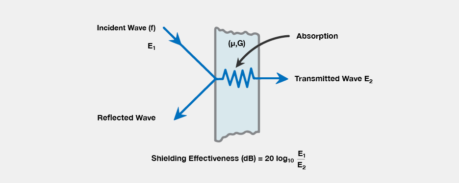
Fig.1
There are many design and analysis tools that can help designers simulate and analyze the radiated emissions even before the hardware is created. Additionally, there are tools and probing techniques that can measure the emissions, both prior to and after shielding has been added.
In addition to the tools, designers need standards with which they can compare their test results to determine if the shielding meets their requirements. See appendix A for a list of most of the shielding standards that are available.
Selecting The Right Shields
In general, designers can address their shielding challenges using a multi-step approach:
- Simulate as much as possible before any physical design.
- Use best PCB design guidelines and ground planes to minimize radiated energy of the prototype design.
- Select components with the appropriate characteristics – size, height, weight, etc.
- Post layout, take extensive radiation measurements to determine where the key sources of emissions are located and the size of the emissions.
- Select the best shielding material and style of shield to minimize the radiated energy.
- Mount the shield and take radiation measurements to verify that the shield performs the desired radiation reduction.
- Convert the prototype to a production-ready version (this may mean adjusting the PCB layout, changing components or other tweaks) and repeat steps 3, 4, 5, and 6.
Shielding Solutions - Many Options
Designers have many shielding options, from the types of materials used in the shields, to the physical structure of the shield itself. Additionally, the material thickness and the continuity of the shield itself also determine how effective the shield will be.
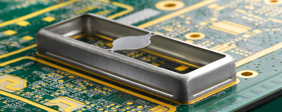
EMI shielding has traditionally been fabricated from metal sheets and formed into structures that surround and cover circuits that either need to be protected or are emitting unwanted radiation.
Steel, copper, and aluminum are viable materials – they are strong and rigid, but if too thin they can deform under the pressures automated handling systems. Once deformed, the metal shields often retain their deformed shape, and that may allow EMI to leak in or leak out of the shield.
When selecting a suitable shielding material there are several aspects that must be addressed:
- The electrical performance (the material’s ability to absorb the EMI/RFI radiation).
- The ability to endure expected environmental conditions (dust, moisture, etc.).
- The mechanical aspects (material behavior such as drawing, bending, cutting, etc.).
- The cost of material and the cost of shaping it and attaching it to the printed circuit board.
RF Shields Manufacturing
RF shields can be formed by bending metal, by casting the metals, or in the case of Masach, by drawing the metal through a mold. Drawing the metal provides a consistent, robust result. The drawn technique yields a seamless shield frame that can withstand handling, transportation, and storage. Snap-on covers complete the shielding assembly.
regarding the shielding materials, as mentioned earlier – shields can be fabricated using steel, brass, nickel, brass, copper, stainless and aluminum. Masach offers pre-tinned steel and brass shields that are readily solderable to PCBs, resulting in considerable cost effectiveness.
Other shield materials would have to be plated post manufacturing. The seamless implementation of drawn shields results in good coplanarity, hence providing a virtual hermetic seal when mounted on a PCB. Additionally, a conductive grommet can be placed between the shield and the cover to close any physical gaps between the elements of the shield, thus minimizing EMI/RFI field leakage.
The drawn process offers designers a level of flexibility – in such that shields of the same X and Y dimensions can have slightly different heights, accommodating alternative component profiles mounted on the PCB. RF Shields can also be formed with or without tabs for pick and place machines, and “mouse” holes in specific positions to enable PCB trace patterns to cross in and out of the shield. Advanced 3D Laser cutting systems employed by Masach can also be used to cut specific openings in the shield to handle out-of-the-ordinary configurations.
RF and EMI Shielding Solutions by Masach
Shielding solutions are available from many sources, and the wide range of surface mountable off-the-shelf options, as well as custom shields from Masach provide a good sampling of what can be delivered. Not only are the many catalog sizes to select from, but to support board-level designs, Masach provides 3D CAD files that can be integrated into production flows.
Full mechanical design* descriptions are also available in PDF data sheets. The data sheets and CAD files are available at https://www.masach.com/products/drawn-rf-shielding-emi-shields.html. Masach also provides support for custom prototyping and small-to-medium production runs. For high-volume production, in-house tooling manufacturing along with automatic press machines supports high-volume requirements.
(a) / (b)
(c) / (d)
Fig.2
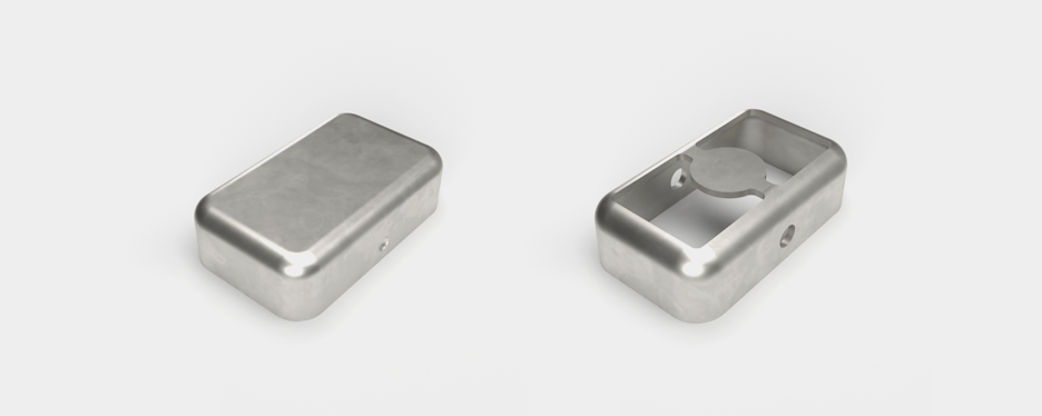
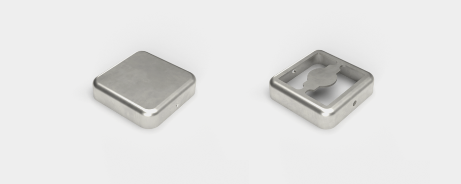
The MS102-10 shields series are fabricated using tin-plated steel or in nickel-silver (Figure 2a and 2b). The choice of metal depends on attenuation and mechanical durability required by the application. A similar choice of metals is available for the MS110-10 shields series (Figure 2c and 2d).
There are many options for using RF shields on PCBs, whether its a two-piece open-frame shield that provides isolation from adjacent components but leaves the top open for access to the components within, or a sealed one-piece shield that blocks all radiated RFI or EMI. View Shields Catalog
Applications that require shields span a wide range of industries such as telecommunications (cell phones, base stations, etc.), medical systems (from pacemakers to magnetic imaging systems), electronic test equipment, avionics, automotive systems, industrial controls, and many other systems.
Let’s examine some real-world examples of how the shields used. In Figure 3, a PCB subsystem operating at 3.2GHz employs multiple open frame and sealed shields to isolate blocks of discreet signal processing circuits from each other yet providing access to the circuits within the open frame shields. The most obvious solution would be to use a multicavity tuner-type shield. However, such a solution has a few issues – for starters, the partition seams between the circuits would require either welding or soldering to limit the emissions. Additionally, at the 3.2-GHz operating frequency, the cover of the surrounding shield should have significant contact with the partition and screen.
Although such a shielding solution works well in many applications, for this particular circuit board, the reduction of RFI/EMI was not sufficient.
To improve the shield effectiveness, designers opted for a shield with no apertures yet providing multiple access routes to each shielded section. An easily removable cover for each module allows for access but when put in place provides the desired EMI/RFI integrity.
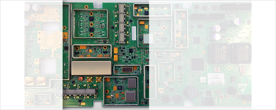
Fig.3
Standard/Custom RFI/EMI Shields For Every Need
Masach can also custom craft shields to suit any size and shape requirement - available from the factory or through one of its worldwide distribution partners. The various metal options also deliver a range of EMI/RFI suppression that meet almost every system need. And, as operating frequencies continue their relentless upward march, more attention must be paid to shielding technologies.
Masach, founded in 1994, is recognized worldwide as a leading supplier of standard and custom drawn shields. The company manages every step of the production cycle, starting with raw materials and design to packaging and shipping, all under one roof. The shields are produced by hydraulic presses, cutting-edge tool room assemblies, Laser trimming and cutting tools and leading-edge forming tools. About Masach Tech
Appendix A
Common shielding effectiveness standards:
• ASTM D 4935-10: Standard Test Method for Measuring the Electromagnetic Shielding Effectiveness of Planar Materials
• ASTM D 4935-99: Standard Test Method for Measuring the Electromagnetic Shielding Effectiveness of Planar Materials
• IEC 61000-5-7: Degrees of Protection Provided by Enclosures Against Electromagnetic Disturbances (EM code)
• IEEE 299-2006: Measuring The Effectiveness Of Electromagnetic Shielding Enclosures
• MIL-DTL-83528C: General Specification For Gasketing Material, Conducting Shielding Gasket, Electronic, Elastomer, EMI / RFI
• MIL-G-83528: General Specification for Gasketing Material, Conducting Shielding Gasket Electronic, Elastomer, EMI / RFI
• MIL-STD 1377: Measurement And Effectiveness Of Cable, Connector, And Weapon Enclosure Shielding And Filters In Precluding Hazards Of Electromagnetic Radiation To Ordnance
• MIL-STD-188-125-1: High-Altitude Electromagnetic Pulse (Hemp) Protection For Ground-Based C4I Facilities Performing Critical, Time-Urgent Missions (Transportable Systems)
• MIL-STD-188-125-2: High-Altitude Electromagnetic Pulse (Hemp) Protection For Ground-Based C4I Facilities Performing Critical, Time-Urgent Missions (Transportable Systems)
• MIL-STD-285: Military Standard For Attenuation Measurements For Enclosures
• MIL-STD-907B: Engineering, Design, And Shielding Effectiveness Criteria For Shelters (Expandable & Non-Expandable)
• IEEE Std 299: Measuring the Effectiveness of Electromagnetic Shielding Enclosures
*Products design and development is certified under ISO 9001 only.
